


Introduction
In semiconductor manufacturing, research, and specialty wafer processing environments, not all wafers conform to traditional round semiconductor packaging formats. Custom Wafer Packaging solutions are specifically engineered to protect non-standard, square, prototype, thin, fragile, and specialty wafers requiring unique handling configurations beyond conventional wafer shipping systems. These packaging assemblies are designed to provide secure transportation, contamination-conscious protection, and precision cushioning for delicate wafer applications where standard packaging solutions may not be suitable.
From square solar wafers and prototype semiconductor substrates to specialized research materials and custom wafer geometries, Custom Wafer Packaging solutions help ensure wafers remain protected throughout storage, handling, manufacturing, and transportation processes.
What is Custom Wafer Packaging?
Custom Wafer Packaging refers to specialized semiconductor wafer handling and shipping solutions designed for wafers that fall outside traditional industry-standard configurations. These packaging systems may incorporate custom foam inserts, specialized wafer jars, square wafer carriers, wafer separators, cushioning assemblies, and engineered protective materials tailored to unique wafer dimensions or application requirements.
Unlike conventional wafer packaging systems designed primarily for standard round silicon wafers, Custom Wafer Packaging solutions accommodate a broader range of wafer types, including square solar wafers, prototype semiconductor wafers, thin or fragile wafers, research and development substrates, specialty material wafers, and non-standard wafer dimensions.
Key Features of Custom Wafer Packaging
Precision Protective Cushioning
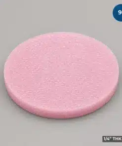
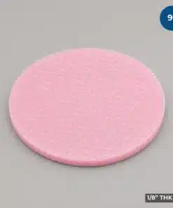
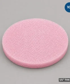
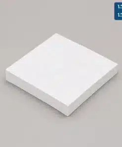
Advanced Foam Protection: Custom foam inserts and engineered cushioning systems securely cradle delicate wafers while reducing movement and vibration during transportation and handling.
Reduced Mechanical Damage: Precision-cut cavities help minimize wafer shifting, edge contact, scratching, and chipping.
Support for Non-Standard Wafer Geometries
Custom Configurations: Custom Wafer Packaging solutions are specifically designed to support square, rectangular, oversized, thin, or uniquely shaped wafers.
Specialized Assemblies: Packaging systems can be configured to accommodate prototype wafers, solar wafers, and specialty semiconductor substrates.
Contamination-Conscious Materials
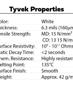
Clean Handling Materials: Packaging materials are selected with semiconductor and electronics handling environments in mind to help minimize contamination risks.
Particle Reduction: Specialized separators, cushioning systems, and wafer supports help reduce particle generation during handling and transportation.
Specialized Wafer Containers and Assemblies
Flexible Packaging Solutions: Custom Wafer Packaging may include specialized wafer jars, custom wafer carriers, foam cushioning systems, interleaf separators, wafer support discs, and prototype packaging assemblies.
Application-Specific Design: Packaging configurations can be adapted to support a wide variety of semiconductor and specialty wafer handling requirements.
Secure Transportation and Handling
Rigid Outer Protection: Durable outer containers help shield wafers from external impacts during storage and transportation.
Internal Stability: Integrated cushioning systems help prevent shifting and vibration that could damage delicate wafers.
Applications of Custom Wafer Packaging
Semiconductor Manufacturing: Supports the handling, storage, and transportation of specialty semiconductor wafers used in manufacturing and process development.
Solar Wafer Applications: Provides protective packaging solutions for square solar wafers and photovoltaic wafer handling applications.
Research and Development: Protects prototype wafers, experimental substrates, and low-volume development materials in laboratory and R&D environments.
Specialty Material Processing: Accommodates fragile substrates and unique wafer materials requiring specialized support and cushioning.
Conclusion
Custom Wafer Packaging solutions provide engineered protection for specialized wafer handling applications that extend beyond traditional semiconductor packaging standards. Combining precision cushioning, contamination-conscious materials, secure transportation features, and flexible packaging configurations, these systems help protect delicate wafers from mechanical damage, particle contamination, and handling risks throughout manufacturing and shipping processes.
Whether supporting square solar wafers, prototype semiconductor substrates, specialty research materials, or unique wafer geometries, Custom Wafer Packaging solutions deliver reliable protection for demanding semiconductor and advanced technology applications.
Protect your specialized wafers with confidence using Custom Wafer Packaging solutions.