
PLCC & LCC
IC Shipping Tubes
Explore antistatic IC shipping tubes for PLCC, leadless LCC, and related chip carrier semiconductor packages. Malaster supplies static-safe tube profiles designed to support package bodies with clearance for PLCC J-leads and LCC terminations, maintain consistent device orientation, and support organized handling through manufacturing, testing, storage, automation, and distribution.
Chip Carrier Protection
Antistatic Shipping Tubes for PLCC & LCC Devices
PLCC and LCC shipping tubes are precision-formed packaging profiles designed to support plastic leaded chip carriers and leadless chip carriers during manufacturing, testing, storage, and transportation. Their internal geometry helps support the package body, maintain consistent device orientation, and reduce unnecessary contact with delicate leads or package edges.
Malaster supplies reusable antistatic tube profiles for a range of PLCC, LCC, and related chip carrier configurations. These static-safe IC shipping tubes support organized handling, automated processing, inventory control, and reliable transport throughout semiconductor manufacturing and distribution.
Why Tube Geometry Matters for PLCC & LCC Packages
Plastic Leaded Chip Carrier (PLCC) packages need body support and clearance around their J-leads. Leadless Chip Carrier (LCC) packages need support that respects package edges, terminations, and permitted contact surfaces. A properly designed IC shipping tube helps control component movement, maintain consistent orientation, and promote smooth loading and unloading during manufacturing, testing, storage, and transportation. Selecting the correct tube profile also improves compatibility with automated handling and inspection processes commonly used throughout semiconductor production.
Common PLCC & LCC Tube Geometries
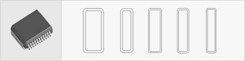
The cross sections below illustrate several common internal profile geometries used for PLCC, LCC, and related chip carrier packages. Actual cavity dimensions, rail geometry, lead clearance, retention features, and device orientation vary by part number. Use the product table below to compare available profiles and review detailed specifications for each tube.
Available PLCC & LCC IC Shipping Tubes
Compare the available antistatic IC shipping tube profiles below. Select any part number to review product dimensions, package compatibility, material information, and other technical specifications for the individual tube.
| Image | Part Number | Product | PRODUCT PAGE |
|---|
Key Features & Common Applications
Malaster antistatic PLCC and LCC IC shipping tubes are designed to provide dependable ESD protection, secure chip carrier handling, and reliable package transport throughout semiconductor manufacturing, testing, storage, and distribution.
Key Features
- Static-safe materials for dependable ESD protection
- Internal geometry supports package bodies and provides clearance for PLCC J-leads or LCC terminations
- Multiple tube profiles for PLCC, leadless LCC, and related chip carrier devices
- Reusable construction for manufacturing and logistics environments
- Compatible with plugs, pins, tube fillers, and bundling accessories
- Custom tube profiles and lengths available for specialized applications
Common Applications
- PLCC and LCC semiconductor device packaging
- Leaded and leadless chip carrier manufacturing and assembly
- Automated pick-and-place preparation
- Electrical testing, inspection, and programming
- Inventory storage and ESD-safe distribution
- Contract electronics manufacturing and worldwide logistics
Why Engineers Choose PLCC & LCC IC Shipping Tubes
PLCC and LCC semiconductor packages require body support and consistent orientation throughout manufacturing, testing, storage, and transportation. PLCC profiles must allow clearance for J-leads; leadless LCC profiles must accommodate package edges and terminations. Properly designed antistatic IC shipping tubes help reduce handling damage, support automated processing, and provide dependable ESD protection from production through final shipment.
Reliable ESD Protection
Static-safe materials help minimize triboelectric charge generation while supporting facility ESD control programs for sensitive chip carrier devices.
Body and Termination Clearance
Internal tube geometry supports the package body and helps limit movement, with clearance for PLCC J-leads or leadless LCC terminations as appropriate.
Multiple Profile Options
Tube profiles are available for PLCC, leadless LCC, and related chip carrier packages to support a broad range of semiconductor applications.
Automation Compatibility
Consistent package orientation supports efficient loading, unloading, inspection, and automated handling throughout manufacturing operations.
Reusable Packaging System
Durable plastic construction supports repeated use throughout manufacturing, inventory management, and global distribution.
Custom Engineering Support
When a standard profile is not the ideal fit, Malaster can evaluate custom tube profiles, lengths, materials, and complete semiconductor packaging solutions.
Build a Complete PLCC & LCC Packaging System
IC shipping tubes are only one part of an effective semiconductor packaging solution. Malaster offers compatible accessories and complementary ESD products that help retain chip carrier devices, manage unused tube space, organize loaded tubes, and support reliable handling throughout manufacturing, storage, and shipment.
Tube End Plugs & Retaining Pins
Secure PLCC and LCC devices inside shipping tubes while helping prevent accidental product loss during handling, storage, and transportation.
Explore Tube Accessories →ESD Rubber Bands
Bundle multiple loaded IC shipping tubes together using reusable static-dissipative rubber bands designed for semiconductor packaging and material handling.
View ESD Rubber Bands →ESD IC Tube Fillers
Fill unused space inside partially loaded tubes to help limit component movement and maintain consistent orientation during handling and shipment.
View IC Tube Fillers →Custom Tube Solutions
When a standard profile does not meet your requirements, Malaster can evaluate custom tube profiles, lengths, materials, and complete semiconductor packaging solutions.
Request a Custom Tube →Choosing the Right Antistatic IC Shipping Tube
Selecting the proper IC shipping tube involves more than matching package dimensions. Learn how tube geometry, ESD materials, lead protection, package orientation, end closures, and tube fillers work together to improve handling, reduce damage, and create a complete semiconductor packaging solution.
Read the Engineering Guide →Need Help Selecting the Right PLCC / LCC Shipping Tube?
For PLCC packages, verify package-body support and clearance around the J-leads. For leadless LCC packages, check package-edge and termination clearance, body dimensions, and permitted contact surfaces. Confirm loading orientation, tube length, and handling-equipment requirements for either package.
Provide Malaster with your component drawing, package dimensions, manufacturer part number, sample device, or existing tube number. We can help identify an available profile or evaluate a custom antistatic tube solution for your PLCC or leadless LCC device.
Submit Your Tube Requirements
Send us your package dimensions, device drawing, estimated quantity, preferred tube length, and any automation or handling requirements. Our team will review the application and help determine the most appropriate next step.
Explore Other IC Shipping Tube Categories
Malaster manufactures antistatic shipping tubes for a wide range of semiconductor package styles. If you’re looking for a different package configuration, explore our additional stock tube categories or contact our engineering team for assistance selecting the correct solution.