

Semiconductor & electronics packaging

Packaging expertise.
Personal attention.

Malaster manufactures and supplies ESD and protective packaging for semiconductor devices, wafers and electronic assemblies. We combine standard products, custom capabilities and hands-on support for fit, materials and handling.

30+ years serving semiconductor packaging customers.

Santa Clara, California

Fit. Materials. Handling. The details belong together.

The Malaster approach

Knowledge beyond
the part number.

Our work brings together manufacturing, product selection and application review. We help customers choose an established package, adapt a component or develop a custom solution around the device and the process.

Start with the device.

We consider support surfaces, lead and contact clearances, retention and loading access. Small differences in device geometry can change which package works.

Plan for real handling.

Materials, temperature exposure, cleanliness, storage and shipping conditions all influence the choice. We review how the packaging needs to work through your process.

Work directly with our team.

Talk through dimensions, material options, quantities and repeat needs with the people involved in quoting, production and order support.
Standard products & custom capabilities

The right approach for your application.

Established packaging formats

A practical starting point.

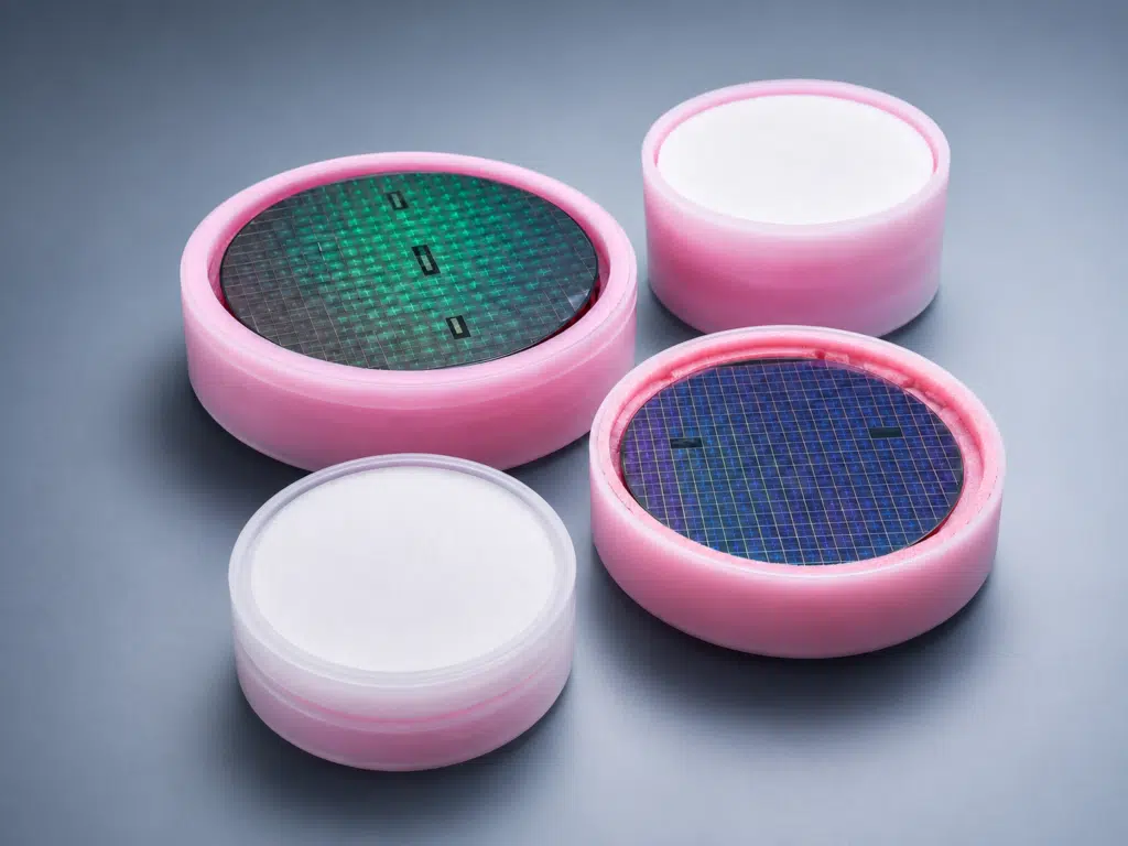
Our range includes IC shipping tubes, JEDEC and thermoformed trays, wafer packaging, protective boxes, ESD bags and accessories. We help match the available options to your device, quantity and handling requirements.

Explore packaging products →

Wafer jars with pink cushions and silicon wafers
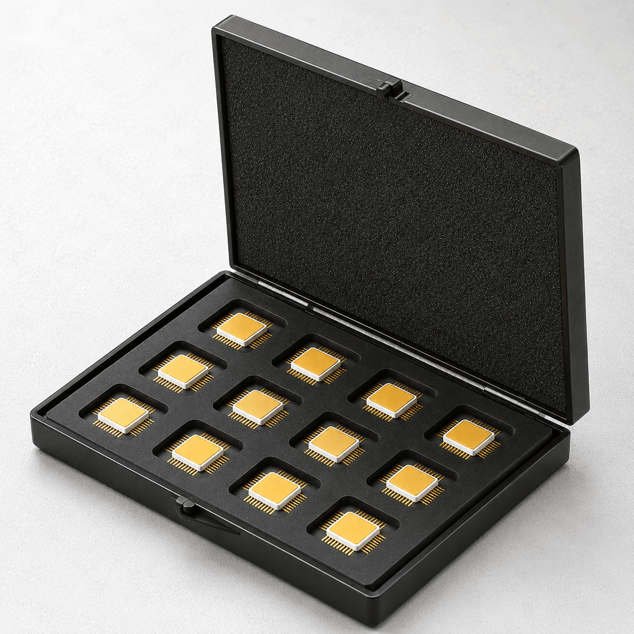
Open conductive device case with semiconductor device and fitted foam insert

Application-specific solutions

When the fit calls
for something different.

When an existing package does not fit, Malaster can develop a custom profile, tray cavity or insert around the device. We review materials, tooling needs, quantities and handling requirements together.

Explore custom packaging →

Put our packaging knowledge to work. Explore guidance on ESD materials, device protection, fit and handling.

Start a conversation

A part number. A drawing.
A packaging problem.

Send the details you have, along with the quantity and timing. Our team can help identify the next step.

Talk with Malaster →

Tell us what you need to protect.