
JEDEC tray sourcing across manufacturers
JEDEC Trays
JEDEC tray options for your device,
your process, and your supply needs.
Malaster helps customers source new trays, requalified reusable trays, replacement options, and custom JEDEC tray solutions across manufacturers. Explore the supply options and package families below, then let the team help narrow the right match.
New trays | Requalified reusable trays | Replacement & custom support
What Malaster can help you source
New, requalified reusable, and custom trays
The right supply option depends on the approved tray design, device fit, condition requirements, quantity, and timing.
New trays
An existing tray design may meet your requirement without new tooling. Availability, material, temperature rating, minimum quantity, and lead time are confirmed for the specific tray.
Requalified reusable trays
Where available and acceptable to your application, previously used trays that have been inspected and prepared for reuse may be an option. Specify your condition and documentation requirements.
Custom tray solutions
When an existing design does not provide the required support or process compatibility, Malaster can help review custom options. Drawings and samples help define cavity geometry and approval requirements.
Have a small requirement or a recurring production need? Include the quantity now, expected ongoing usage, and your needed-by date. The supply recommendation starts with those details.
Explore common applications
Tray options for a range of device packages
Malaster reviews tray requirements across these package families. The full device geometry determines which designs are suitable within each family.
BGA & LGA trays
Tray options for area-array devices, with package support and clearance around sensitive underside features.
QFP, TQFP & MQFP trays
Tray designs for leaded packages, with cavity geometry that supports the package body and accommodates the leads.
QFN & DFN trays
Options for compact leadless devices, where body size, thickness, and underside contact areas influence the cavity.
TSOP & PLCC trays
Matrix tray designs for established package families, including replacement and legacy tray requirements.
PGA trays
Tray options that account for pin geometry, package support, orientation, and the way devices will be handled.
Special device & custom requirements
Existing or custom tray options for unusual geometry, sensitive contact areas, modules, and application-specific handling.
These examples describe sourcing options. Current availability, quantities, material, and tray condition are confirmed for the specific requirement.
From tray options to the right match
Why Malaster reviews the match before quoting
A tray list can show a package name or molded number. It cannot, by itself, confirm that the available tray supports your device, mates with your existing stack, or meets your process requirements. Similar-looking trays may have different cavities, revisions, materials, or temperature capabilities.
Malaster works across manufacturers to review an existing design, a compatible alternative, requalified reusable supply, or a custom option. The recommendation also depends on the condition, quantity, and timing you need.
Already know the tray you need? Go straight to the request page with the complete identifier and quantity. If you are still exploring, the guidance below can help you understand the options before contacting the team.
Check Options for Your TrayPractical support from Malaster
Experience with the tray
and the application.
Malaster’s team includes experience working for a JEDEC tray manufacturer, along with day-to-day work helping customers identify and source trays. That experience helps the team interpret existing trays and review suitable options across manufacturers.
See how Malaster approaches tray identificationWhen you are ready
Choose your next step
01 / Existing tray
Replace a tray you already use
Send complete tray photos, every molded marking, and the device information. Include revision letters and temperature markings so the replacement search starts with the full picture.
See the identification checklist02 / New device
Find a tray for your device
Share the package drawing, device part number, quantity, and handling requirements. Malaster can review existing tray designs against your device and process.
Review the fit considerations03 / Custom requirement
Discuss a custom solution
Unusual geometry, sensitive contact areas, or process requirements may call for a custom cavity or tray. Send what the device needs to do and where it needs support.
Discuss your tray requirementsApplication review
A package name is a starting point. Fit decides.
BGA, QFP, QFN, LGA, PGA, PLCC, and TSOP describe package families. The full device drawing and application requirements determine which tray designs deserve review.
Device fit & contact
Body dimensions, lead or ball geometry, package height, and sensitive contact areas determine how the device should sit in the cavity.
Orientation & equipment
Pin-one orientation, pickup access, cavity positions, and tray condition need to suit the handling equipment and process.
Stacking & covers
Confirm that mating trays align and retain the device correctly. Include the required empty top tray or approved cover configuration.
Temperature & exposure
Provide the actual temperature, time, and repeat-cycle requirements. Tray color alone does not establish material or bake suitability.
ESD & cleanliness
Specify the electrical performance, cleanliness, and documentation your application requires, especially when considering reusable trays.
Quantity & timing
Include initial quantity, ongoing demand, and the date needed. Count the empty cover trays required for the planned stacks.
Same JEDEC outline does not mean interchangeable. The outside format supports common handling systems, while cavity geometry, device support, revisions, and stacking details can differ. A familiar part number or matching package family still needs review.
Identify an existing JEDEC tray
A few good photos can move the search forward.
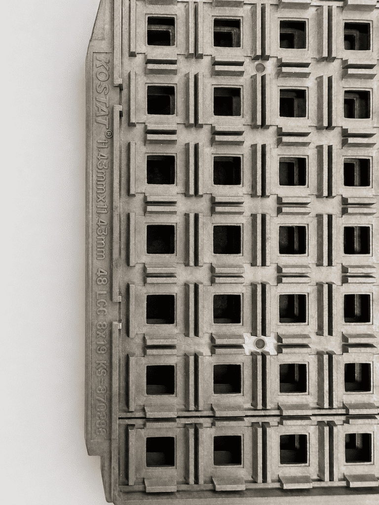
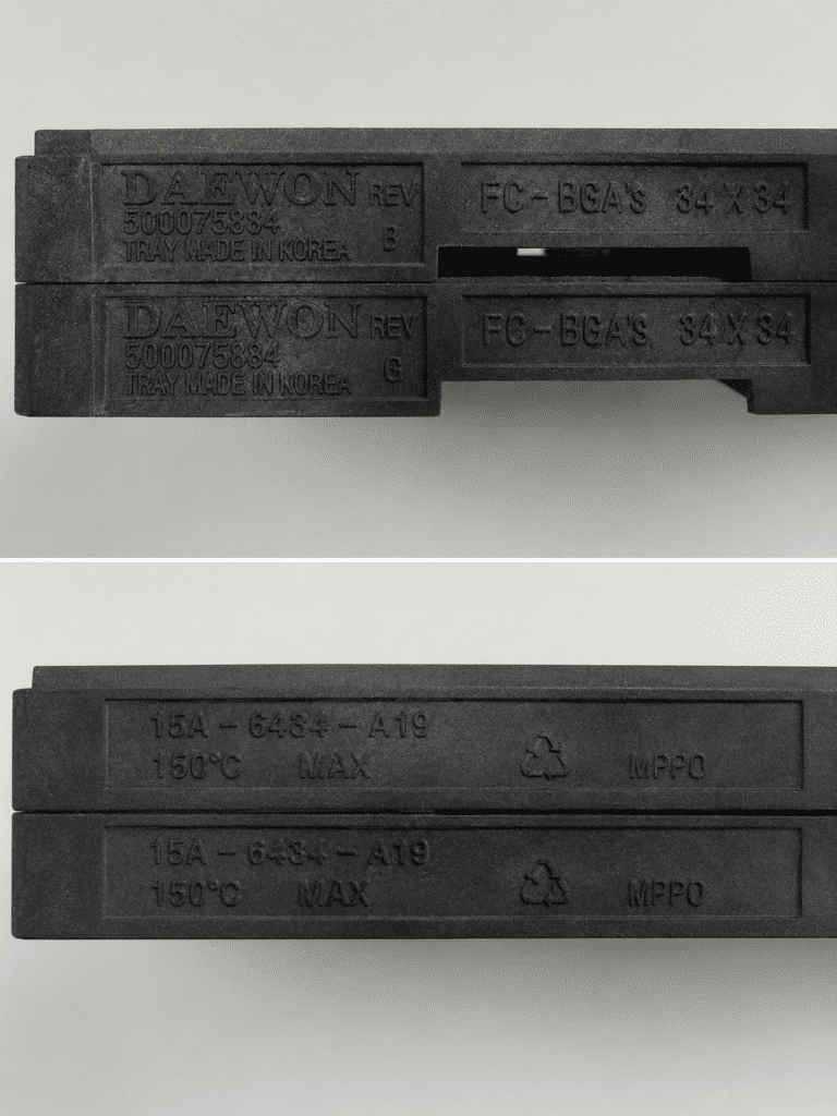
Photograph
- The complete top and bottom of the tray.
- Both end tabs and every molded number, letter, logo, and temperature mark.
- The device correctly seated in a cavity, if available.
Include with the photos
- The device manufacturer, full part number, and package drawing.
- Required tray quantity, needed-by date, and cover-tray needs.
- Any bake temperature and duration, automation requirements, or condition restrictions.
Keep an existing tray and device sample available when fit or revision is uncertain. Clear photographs are a starting point; some applications need physical fit review.
Read the complete tray-identification guideReady to take the next step?
Request help with a tray, replacement, or new application
Use the JEDEC Tray Request page to send what you have available and describe the requirement. It brings the request form, helpful checklists, and next-step guidance together.
A tray number, photograph, or device drawing can be enough to start the conversation. The team can help identify what still needs to be confirmed.
Complete the packaging
Plan the cover, retention, and outer protection.
A tray is one part of the shipping or handling system. Tell Malaster how the loaded stacks will be secured and protected.
Covers & tray stacks
Account for a matching empty top tray or the approved cover arrangement. Confirm that the cover retains the device as required; a dust cover may serve a different purpose.
Include covers in your inquiryESD straps & bands
Select a suitable fastening method that keeps the stack aligned without distorting the trays. Malaster offers reusable ESD hook-and-loop straps and ESD rubber bands.
Browse ESD Velcro strapsCompare ESD rubber bands
Bags & shipping protection
Select the bag for the required shielding or moisture protection, then protect the stack against movement and impact in the shipping carton.
Review ESD bag optionsCommon purchasing questions
Before you request a tray
Select a question to open or close its answer.
Can you help if I only have a molded tray number?
Yes. Send the number and clear photographs of the full tray and both ends. The manufacturer, revision, material markings, and device information help narrow the search; the main number alone may not settle the match.
Do you offer small quantities?
Send the quantity you need. Minimum quantities and availability depend on the tray design, condition, material, and supply option. An existing or requalified reusable tray may be worth reviewing before a custom option.
What affects the price and lead time?
The specific design, material, condition, quantity, availability, and any custom work all matter. Malaster confirms pricing and timing against the reviewed requirement rather than applying one price or lead time to every JEDEC tray.
Will I need to send a physical sample?
Photographs and a complete drawing may be enough for an initial review. Tray and device samples can be needed when the fit is critical, the package is unusual, or the revision and contact geometry are uncertain.
Continue your technical review
Identify an existing tray
Photographs, markings, revisions, and the device details that help the search.
Read the identification guideGo deeper on tray requirements
Materials, cavity design, ESD performance, inspection, handling, and reuse.
Explore the JEDEC Tray Technical HandbookJEDEC Tray FAQ
Practical answers about selection, replacements, process requirements, and sourcing.
Read the JEDEC Tray FAQNew or requalified trays?
Compare condition, application approval, documentation, and supply planning.
Compare new and requalified traysHave a tray, drawing, or device requirement?
Let’s Review Your JEDEC Tray Needs