
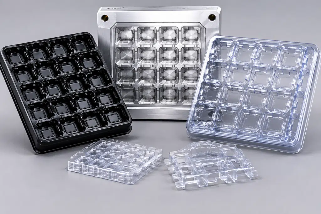
01 / Custom services
Start with the packaging you need.
Go directly to a service or request form. If the project involves several components, start with a packaging consultation.
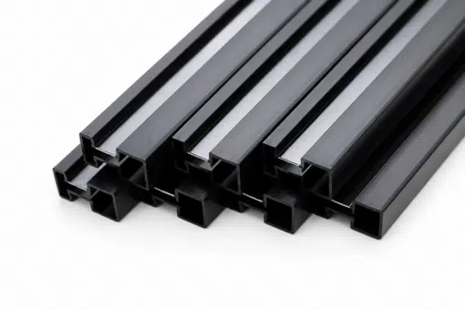
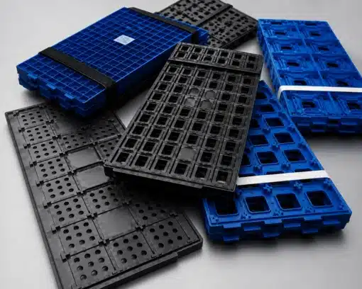
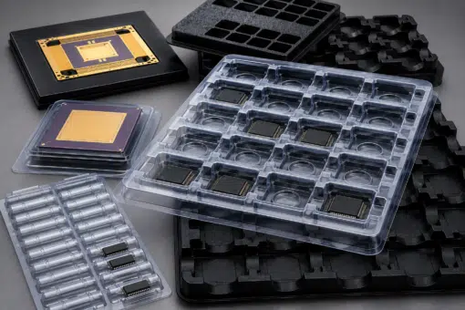
02 / Application review
The details that determine the design.
A package must support the device through loading, processing, storage and shipment. Malaster reviews the requirement across those steps so the proposed components work together.
Fit & contact
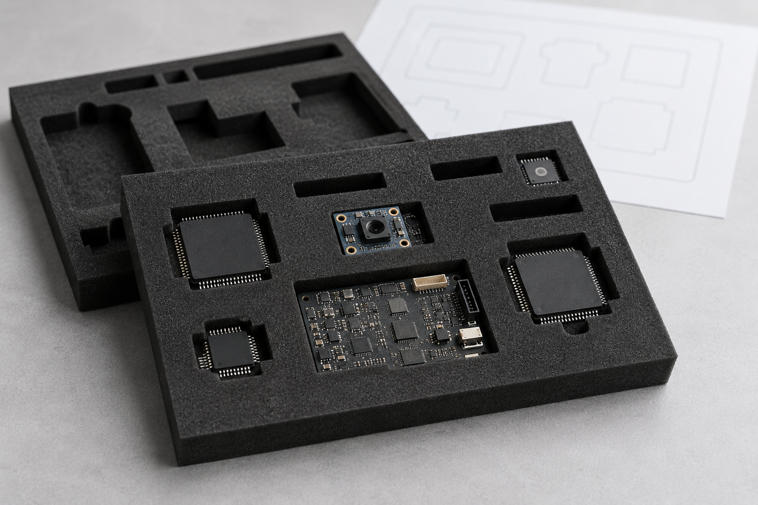
Identify the support surfaces, fragile features, lead or ball clearances, and the movement the package must control.
Handling & environment
Define orientation, pickup access, stacking, temperature exposure, cleanliness and any manual or automated handling requirements.
Protection & materials
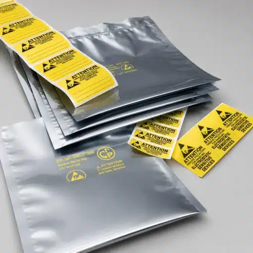
Specify the electrical behavior, cushioning and moisture protection required. Review technical data against the actual application.
An existing format may be the right starting point.
We review whether a standard package, a modified component or a new design fits the requirement. An existing format may help avoid unnecessary tooling, subject to fit and availability. For smaller orders, see our guide to low-minimum custom ESD packaging.
03 / Development process
From a packaging problem to a defined requirement.
The first review establishes what is known, what needs to be confirmed and which packaging approach deserves a closer look.
01
Define the application
Share the device, existing packaging and the problem to solve. We review geometry, handling and protection requirements.
02
Review the approach
Compare an existing format, a modification or a custom concept. Identify material choices and details that still need confirmation.
03
Confirm the next steps
Review drawings, sample or fit-check needs, tooling, quantities and timing for the proposed solution before production planning.
04 / Project checklist
Send what you have. We can help fill in the gaps.
You do not need a finished specification to begin. These details make the initial review more useful.
Device & dimensions
Package drawing, part number, critical dimensions and areas that must remain free of contact.
Current packaging
Photos, markings, known issues and any available device or packaging samples.
Process & protection
Loading method, handling equipment, ESD requirements, cleanliness, temperature and shipping conditions.
Quantity & schedule
Initial quantity, expected repeat demand, target date and any sample or approval requirements.
05 / Common questions
Before you request a custom solution.
Does custom packaging always require new tooling?
No. An existing format or a modified component may meet the need. Tooling requirements depend on the reviewed design and manufacturing approach.
Can you work from a photograph or sample?
Yes. Photos, device drawings and existing packaging can support the initial review. Critical dimensions and physical fit may still need to be confirmed.
What affects minimum quantity and lead time?
Material, dimensions, manufacturing method, tooling and approval requirements all matter. Include the quantity and needed-by date so Malaster can review a practical supply option.
How is the ESD material selected?
Low-charging, dissipative, conductive and shielding describe different behaviors. Selection starts with the device and handling requirements, then the relevant material and packaging data. Read the ESD fundamentals guide →
What if my project uses several packaging components?
Use the general consultation request. Describe the full arrangement, including the carrier, insert, cushioning, bag and retention method, so the components can be reviewed together.