
Conductive Device Inserts
Conductive device inserts securely retain semiconductor components, integrated circuits, and precision electronic devices inside conductive ESD shipping boxes. Available in standard package outlines or custom engineered designs, Malaster insert systems provide reliable protection using either conductive foam or precision molded lid inserts for sensitive semiconductor packaging applications.
Conductive Device Inserts for Semiconductor Packaging
Conductive device inserts for semiconductor packaging are precision thermoformed to securely retain integrated circuits, semiconductor components, and other static-sensitive electronic devices inside conductive ESD shipping boxes. By positioning each device within a dedicated cavity, these reusable inserts help reduce movement during storage, handling, and transportation while supporting reliable electrostatic discharge protection.
Malaster offers standard inserts for common semiconductor package configurations, precision foam-free retention systems, and fully custom conductive packaging solutions. A California company since 1993, Malaster can help identify an insert and protective packaging approach suited to your component dimensions, handling requirements, and distribution environment.
Choose the Right Packaging Solution
Malaster offers several conductive packaging approaches depending on your device, handling requirements, and level of protection needed.

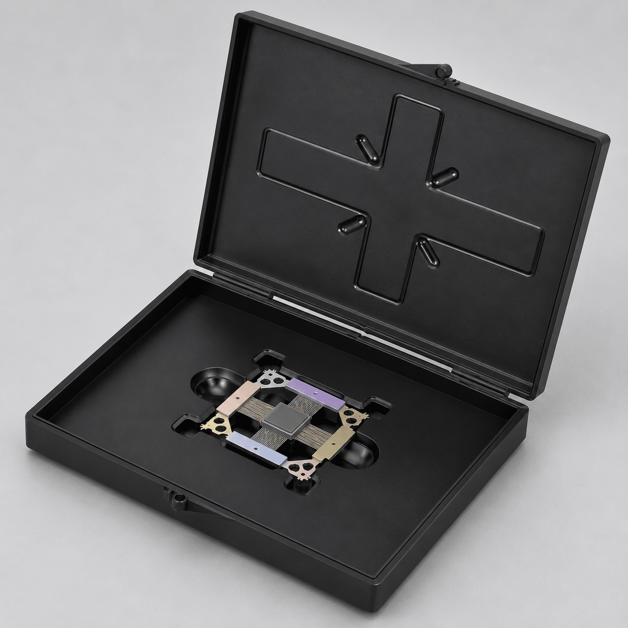

Standard Conductive Device Inserts
Browse Malaster’s library of standard conductive device inserts for many common semiconductor package styles. Use the filters below to quickly locate an existing insert by package family or conductive box series. If your device package is not listed, our engineering team can design a custom conductive insert tailored to your application.
| Image | Part Number | Product | Package Style | Box Series | PRODUCT PAGE | hf:tax:pa_package-style | hf:tax:pa_esd-box-series |
|---|
Need a Custom Conductive Device Insert?
If your semiconductor package isn’t represented in our standard insert library, Malaster’s engineering team can develop a custom conductive device insert tailored to your device geometry, handling requirements, and packaging objectives. From prototype development through production tooling, we create precision ESD-safe packaging solutions designed specifically for your application.
Whether you need a custom thermoformed insert, a precision lid retention system, or a complete conductive packaging solution, we’re ready to help.