Featured Selection Guide
Choosing the Right Antistatic IC Shipping Tube
Understand how package dimensions, lead geometry, tube profile, material properties, accessories, and order requirements influence proper tube selection.
Read the Guide
Semiconductor Device Packaging
Practical guidance for selecting, specifying, handling, and using antistatic IC shipping tubes. Explore tube profiles, material properties, device fit, accessories, shipping considerations, and application support for sensitive semiconductor components.
Topic Overview
Jump directly to the part of IC shipping-tube selection or application guidance that is most relevant to your work.
Reliable Device Protection
IC shipping tubes provide a practical way to organize, protect, store, and transport sensitive semiconductor devices while maintaining orientation and reducing uncontrolled movement.
Their long, repeatable profile makes them especially useful for component handling, manual assembly, inventory storage, shipment, and applications where devices must remain aligned throughout the packaging process.
The correct tube depends on more than package name alone. Device dimensions, lead geometry, profile clearance, material behavior, loading direction, accessories, and shipping conditions all affect whether a tube will perform as intended.
Technical Learning Library
Explore practical guidance covering tube selection, packaging-format comparisons, materials, accessories, device compatibility, and shipping considerations.
Featured Selection Guide
Understand how package dimensions, lead geometry, tube profile, material properties, accessories, and order requirements influence proper tube selection.
Read the GuidePackaging Comparison
Compare common semiconductor packaging formats based on device geometry, loading, automation, storage, shipping, and handling requirements.
Read the ComparisonTube Packaging Overview
Review the practical role IC shipping tubes play in component organization, orientation, protection, storage, and transportation.
Read the OverviewFuture Technical Guide
Learn how electrical behavior, application conditions, and handling requirements influence material selection for IC shipping tubes.
Resource in DevelopmentAccessories and Retention
Explore accessories used to retain devices, close tube ends, separate components, and manage unused space inside shipping tubes.
Explore Tube AccessoriesShipping and Handling Guide
Review five practical checks for shipping loaded IC tubes, including tube retention, cushioning, shielding-bag closure, ESD notices, and safe receiving.
Read the five shipping checks →Device Package Families
Tube profiles are designed around the geometry, lead configuration, orientation, and clearance requirements of specific semiconductor package families.

Dual In-Line Packages
Tube profiles designed to protect and orient dual in-line packages while providing clearance for body dimensions and through-hole leads.
Explore DIP Tubes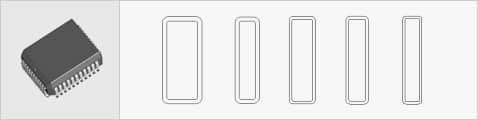
Leaded Chip Carriers
Profiles intended to support square or rectangular plastic leaded chip carriers while limiting movement and protecting perimeter leads.
Explore PLCC Tubes
Leadless Device Packages
Tube configurations for compact leadless packages where body fit, orientation, movement control, and surface protection are critical.
Explore QFN Tubes
Small Outline Packages
Profiles for small-outline integrated circuits that help protect device leads while maintaining consistent orientation during handling and shipment.
Explore SOIC and SOJ Tubes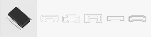
Small Outline Packaging
Tube profiles selected around component width, body height, lead geometry, loading direction, and handling requirements.
Explore SOP Family Tubes
Transistor Outline Packages
Specialized profiles for transistor-outline devices, sockets, and related components requiring secure orientation and lead protection.
Explore TO and Socket Carrier TubesDevices within the same package family may vary in body dimensions, lead geometry, height, orientation, and required clearance. Confirm actual component dimensions or provide a sample before selecting a tube profile for a new application.
Engineering Process
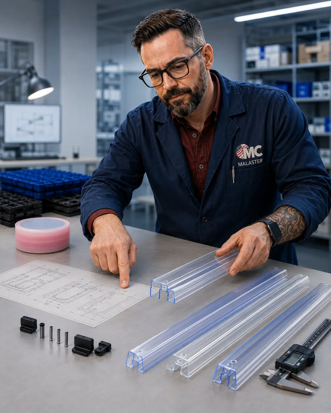
Choosing the correct shipping tube is more than matching a package name. Experienced application engineers evaluate the device, tube profile, material, accessories, and shipping requirements together to ensure reliable handling and protection.
Package style and dimensions
Select the correct cavity
Choose proper ESD properties
Plugs, pins and fillers
Packaging and transportation
Confirm the actual body dimensions, lead configuration, overall height, and orientation. Package family alone rarely guarantees compatibility.
Select a profile that provides appropriate clearance while preventing excessive movement during handling and transportation.
Material selection depends on the application’s electrical requirements, environmental conditions, and ESD protection objectives.
End plugs, pins, fillers, and retaining accessories help keep devices secure while maximizing tube performance.
From MC’s Workbench
“Package families are where we begin. Dimensions are where we make the right decision.”
One of the most common mistakes engineers make is assuming every DIP, SOIC, or QFN device fits the same shipping tube. Small differences in body width, lead geometry, package height, and molding variations can determine whether a component is properly protected or vulnerable to movement during shipment.
Whenever possible, provide a mechanical drawing when requesting a new tube recommendation. If drawings are unavailable, sending a sample device allows us to verify fit before production and eliminate costly packaging issues later.
After reviewing thousands of semiconductor packaging applications, I’ve learned that spending a few extra minutes selecting the correct tube profile almost always saves hours of troubleshooting after shipment.