
Antistatic & Conductive
IC Shipping Tubes
Explore Malaster’s extensive selection of antistatic and conductive IC shipping tubes for semiconductor packaging. We supply ESD-safe tube profiles for DIP, SOIC, PLCC, QFN, TSOP, TO, socket carrier, and other integrated circuit package families, including stocked profiles, low-quantity ordering, and custom tube solutions for automated handling, storage, manufacturing, and transportation.
Compare IC Shipping Tubes by Package Type
Select an IC shipping tube family below to compare available tube profiles, integrated circuit package compatibility, technical specifications, and ESD protection options. Malaster supplies antistatic and conductive tube solutions for semiconductor manufacturing, electronics assembly, automated handling, storage, and transportation of static-sensitive components.
Malaster supplies one of the industry’s broadest selections of antistatic and conductive IC shipping tubes for semiconductor packaging. Our tube profiles support DIP, SOIC, PLCC, QFN, TSOP, TO, socket carrier, optoelectronic, and power semiconductor applications, along with custom tube designs for specialized devices and handling requirements. Each solution is engineered to improve ESD protection, component alignment, automated equipment compatibility, storage efficiency, and transportation reliability throughout the manufacturing and distribution process.
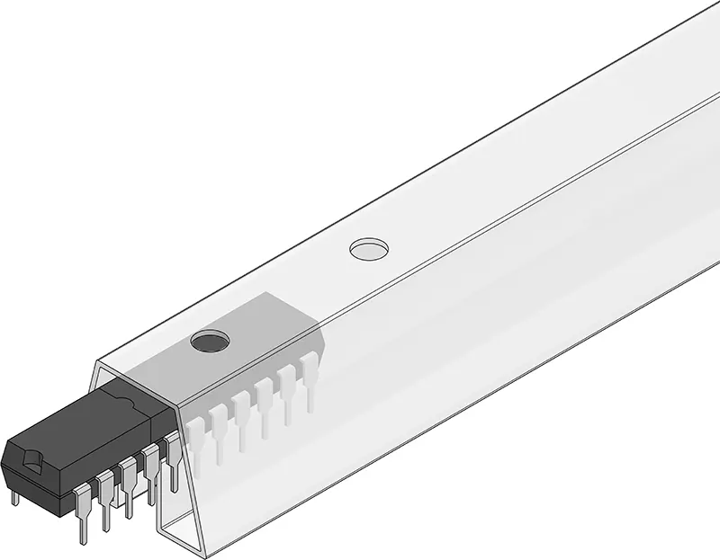
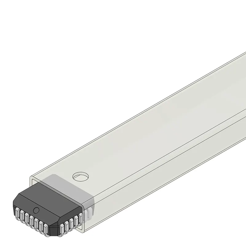
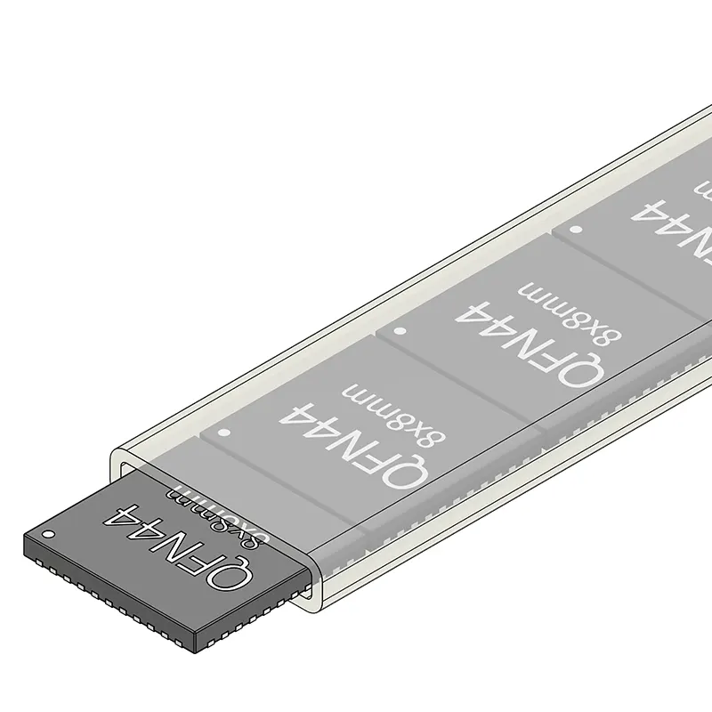


Two semiconductor packages with similar body dimensions may still require different IC shipping tube profiles. Lead geometry, maximum lead span, package height, molding tolerances, component orientation, and downstream automation equipment can all affect how a device fits and travels through a tube. Selecting a profile based only on package width can result in poor alignment, damaged leads, device rotation, or inconsistent feeding. The complete component geometry and intended handling process should be evaluated when selecting an antistatic or conductive tube profile.
For a closer look at fit and handling, read the IC tube selection guide or explore the IC shipping tube technical guides.
Why Engineers Choose Antistatic & Conductive IC Shipping Tubes
IC shipping tubes are designed to protect semiconductor devices throughout manufacturing, storage, and transportation while supporting efficient handling and automation. Their combination of ESD protection, physical protection, and standardized profiles makes them one of the most widely used packaging solutions in the electronics industry.
Reliable ESD Protection
Antistatic and conductive materials help minimize triboelectric charge generation and support ESD control programs for static-sensitive semiconductor devices.
Consistent Device Orientation
Individual tube profiles maintain proper component alignment for manual handling, automated feeding, inspection, and downstream manufacturing processes.
Physical Component Protection
Tube packaging helps reduce bent leads, package damage, contamination, and handling-related defects during storage and transportation.
Automation Compatible
Standardized tube profiles integrate with automated loading, unloading, inspection, test, and packaging equipment used throughout semiconductor manufacturing.
Reusable Packaging
Durable tube construction allows packaging to be reused throughout manufacturing, inventory management, distribution, and customer returns where appropriate.
Broad Package Compatibility
Available for DIP, SOIC, SOJ, SOP, TSOP, TSSOP, PLCC, LCC, QFN, TO packages, socket carriers, power semiconductors, optoelectronics, and many specialty devices.
Complete IC Shipping Tube Packaging Solutions
An IC shipping tube is often only one part of a complete semiconductor packaging system. The tube profile protects and organizes the device, while properly selected closures, restraints, cushioning, and outer packaging help secure components throughout manufacturing, storage, internal movement, and shipment.
Malaster supplies compatible packaging components that can be combined into a coordinated ESD-safe solution, reducing the need to source critical items from multiple suppliers while helping maintain consistent protection throughout the handling process.
Tube Plugs & End Stops
Conductive plugs, end stop pins, and fillers help retain devices inside the tube while supporting loading, storage, and shipment.
ESD Rubber Bands
Antistatic rubber bands help bundle tubes together and reduce unnecessary movement during storage, handling, and transportation.
Conductive Storage Boxes
Conductive and static-dissipative boxes provide organized secondary containment for tubes and sensitive semiconductor components.
ESD Foam & Cushioning
Antistatic, conductive, and static-dissipative foam can cushion tubes, control movement, and provide additional protection inside outer packaging.
By evaluating the complete packaging system rather than the tube alone, manufacturers and distributors can improve device protection, simplify procurement, and create a more consistent process from production through final delivery.
Let’s Find the Right IC Shipping Tube for Your Application
Selecting the correct IC shipping tube requires more than matching the package body dimensions. Maximum lead span, package height, lead configuration, component orientation, profile clearance, material requirements, automation compatibility, and transportation conditions can all affect tube performance.
Whether you are replacing an existing tube, qualifying packaging for a new semiconductor device, or evaluating a custom profile, Malaster can help review the application and identify an appropriate stocked or non-stock solution.
For non-stock or custom tube requirements, submit the available device drawing, package dimensions, existing tube number, sample information, estimated quantity, and application details through our custom tube request form. The more information provided, the more efficiently we can evaluate potential profile options.