

ESD Packaging Resources, Foundational Guide
ESD Packaging Guide: How to Protect Sensitive Electronic Components
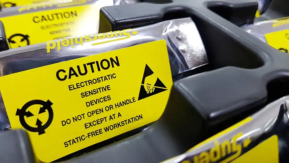
Jun
Electrostatic discharge can damage sensitive electronic components during handling, storage, assembly, and transportation. Some ESD events cause immediate failure, while others create latent damage that may not appear until the component is operating in the field. The correct packaging system must therefore provide both electrical protection and physical protection appropriate to the component, handling process, and shipping environment.
This guide explains the primary functions of ESD packaging, the differences between low-charging, static-dissipative, conductive, and shielding materials, and the practical factors to consider when selecting packaging for semiconductors, circuit boards, wafers, and other sensitive electronic devices.

Table of Contents
- What Is Electrostatic Discharge?
- How ESD Damages Electronic Components
- What ESD Packaging Must Do
- ESD Packaging Material Types Compared
- Packaging Inside and Outside an ESD Protected Area
- Choosing the Right ESD Packaging Format
- Factors to Evaluate Before Selecting Packaging
- Common ESD Packaging Selection Mistakes
- ESD Packaging Selection Checklist
- Protecting Components with the Right Packaging System
What Is Electrostatic Discharge?
Electrostatic discharge, commonly called ESD, is the rapid transfer of electrical charge between objects at different electrical potentials. Charge can accumulate through contact and separation between materials, movement across surfaces, handling by personnel, or interaction with equipment and packaging.
An ESD event may occur when a charged person, tool, container, or material contacts an electronic device. The discharge can happen too quickly to be seen or felt, yet still exceed the withstand voltage of a sensitive semiconductor component.
Because charge generation depends on the materials, humidity, movement, grounding, and surrounding environment, ESD control requires more than choosing a package labeled “antistatic.” The packaging must be selected as part of the complete handling and transportation process.

How ESD Damages Electronic Components
ESD damage generally appears in one of three ways:
- Catastrophic failure: The component no longer functions after the ESD event.
- Latent damage: The component continues to operate but has been weakened, potentially reducing its service life or reliability.
- Intermittent performance: The damage creates inconsistent behavior that can be difficult to reproduce and diagnose.
The business impact can extend beyond the value of the individual component. ESD-related failures may cause production delays, troubleshooting costs, rework, warranty claims, field failures, and damage to customer confidence. These risks are especially important in semiconductor manufacturing, aerospace, defense, medical electronics, automotive systems, telecommunications, and other applications where component reliability is critical.
What ESD Packaging Must Do
A complete ESD packaging system may need to perform several different functions. These functions are related, but they are not interchangeable.
Reduce Charge Generation
Low-charging materials are designed to reduce triboelectric charge generation when materials contact, separate, rub, or move against one another. This property is often described as antistatic. Low charge generation is important, but it does not by itself guarantee charge dissipation or shielding.
Control Charge Movement
Static-dissipative and conductive materials allow electrical charge to move across or through the material. The appropriate resistance range depends on the application and the requirements of the ESD control program. These materials must be used within a properly designed system; packaging does not automatically become grounded merely because it is conductive.
Provide Electrostatic Discharge Shielding
Shielding packaging limits the energy that can reach the contents when an electrostatic discharge occurs outside the package. This is particularly important when sensitive items leave a controlled ESD protected area and enter an uncontrolled shipping, storage, or customer environment.
Prevent Physical Damage
Electrical protection is only part of the packaging requirement. The package must also protect leads, surfaces, wafers, terminals, and other delicate features from impact, vibration, abrasion, bending, contamination, and movement. Packaging that provides suitable electrical properties but allows the component to shift or contact damaging surfaces may still be the wrong solution.
ESD Packaging Material Types Compared
| Material Function | Primary Purpose | Important Limitation | Typical Packaging Uses |
|---|---|---|---|
| Low-charging / antistatic | Reduces charge generation caused by contact and separation. | Does not necessarily provide controlled dissipation, conductivity, or discharge shielding. | Bags, liners, cushioning, temporary handling materials, and packaging for appropriate controlled applications. |
| Static-dissipative | Allows charge to move and decay at a controlled rate. | Does not automatically provide a shielding barrier against an external ESD event. | Trays, tubes, containers, cushioning, work-in-process packaging, and component carriers. |
| Conductive | Allows charge to move readily across or through the material and helps equalize potential within a controlled system. | Must be selected and used correctly; conductive material alone does not guarantee grounding or shielding. | Component trays, conductive boxes, tube plugs, carriers, and reusable handling containers. |
| Discharge shielding | Reduces the energy reaching the packaged item during an external electrostatic discharge. | The interior packaging must still provide suitable contact, cleanliness, mechanical, and low-charging properties. | Shielding bags, layered packaging systems, and transport packaging used outside controlled ESD areas. |
The correct material cannot be selected by color or by a single marketing term. The electrical properties should be verified against the component sensitivity, intended use, applicable standards, and the organization’s ESD control plan.
Packaging Inside and Outside an ESD Protected Area
An ESD protected area, often abbreviated EPA, is a controlled environment in which personnel, equipment, work surfaces, grounding, and materials are managed to reduce ESD risk. Packaging used entirely inside an EPA may have different requirements from packaging used for shipment outside that controlled environment.
Inside an ESD Protected Area
Inside an EPA, packaging often needs to minimize charge generation and provide suitable conductive or static-dissipative properties where it contacts the component. The packaging must also work with the facility’s grounding, handling, and process controls.
Outside an ESD Protected Area
Once a component leaves an EPA, it may be handled by carriers, warehouse personnel, customers, or automated systems in uncontrolled conditions. In those situations, the packaging system may also need discharge shielding and stronger physical protection.
This distinction is important because a package that performs adequately inside a controlled production area may not provide sufficient protection during transportation or customer handling.
Choosing the Right ESD Packaging Format
The package format should support the geometry, sensitivity, quantity, handling method, and destination of the component. Malaster supplies and develops several types of protective packaging for semiconductor and electronics applications.
Conductive and ESD Protective Boxes
ESD protective boxes provide reusable containment for components, assemblies, circuit boards, and other sensitive items. Conductive or static-control foam can be added when the application requires positioning, cushioning, lead protection, or separation between parts.
Thermoformed ESD Trays
Thermoformed ESD trays can hold components in defined orientations for handling, storage, shipping, presentation, or automated processes. The cavity geometry, material thickness, component clearances, nesting, denesting, and handling method all affect tray performance.
IC Shipping Tubes
ESD and antistatic IC shipping tubes are commonly used for linear component storage, transportation, and automated feeding. Tube selection must account for the component profile, lead configuration, orientation, length, end closures, and required electrical properties.
JEDEC Tray Solutions
JEDEC tray solutions support standardized handling and processing of integrated circuits. Proper tray selection requires matching the package style, body dimensions, lead configuration, matrix, temperature requirements, and processing environment.
ESD Foam and Cushioning
ESD foam cushions and inserts can protect parts from shock, vibration, abrasion, and movement while providing the electrical properties required by the application. Foam density, cell structure, compression, cleanliness, thickness, and recovery characteristics should all be considered.
Custom ESD Packaging
Standard packaging is not always suitable for unusual component geometries, delicate surfaces, automated handling, or specialized shipping requirements. A custom packaging solution may combine trays, foam, boxes, tubes, separators, and other components into a system designed around the part and process.

Factors to Evaluate Before Selecting ESD Packaging
Before choosing a material or package format, evaluate the complete use case rather than only the component dimensions.
- Component sensitivity: Determine the device’s ESD sensitivity and any customer-specific handling requirements.
- Handling environment: Identify whether the package will remain inside an EPA or travel through uncontrolled environments.
- Component geometry: Consider body dimensions, leads, terminals, delicate surfaces, protrusions, and allowable contact areas.
- Mechanical risks: Evaluate shock, vibration, abrasion, compression, bending, and movement during handling and shipment.
- Cleanliness requirements: Consider particle generation, outgassing, contamination sensitivity, and compatibility with clean processes.
- Packaging life cycle: Determine whether the package is disposable, returnable, reusable, washable, or expected to withstand repeated handling.
- Process compatibility: Account for automation, conveyors, robotic handling, baking, inspection, stacking, labeling, and storage.
- Transportation conditions: Consider carrier handling, temperature, humidity, package orientation, shipment duration, and secondary packaging.
- Applicable standards: Document packaging requirements as part of the ESD control program and consider applicable guidance such as ANSI/ESD S20.20, IEC 61340-5-1, and ANSI/ESD S541.
Common ESD Packaging Selection Mistakes
Assuming “Antistatic” Means Complete ESD Protection
Antistatic or low-charging material helps reduce charge generation, but it may not provide the dissipation or shielding required for a sensitive component. The term should not be treated as a complete specification.
Selecting Electrical Properties but Ignoring Mechanical Protection
A component can be electrically protected and still be damaged by impact, movement, lead deformation, abrasion, or excessive compression. The packaging must address both hazards.
Using Packaging Designed for an EPA During Uncontrolled Transportation
Packaging that works well inside a controlled facility may not provide sufficient discharge shielding once it enters a carrier network, warehouse, or customer location.
Allowing Packaging to Contact the Wrong Component Features
A cavity, tube, foam insert, or separator should support the component at appropriate surfaces. Contact with fragile leads, wire bonds, polished surfaces, or sensitive edges can cause damage even when the package fits dimensionally.
Choosing by Color Alone
Pink, black, blue, clear, or metallic appearance does not by itself establish the electrical performance of a packaging material. Material properties and supplier documentation should be reviewed for the intended application.
Overlooking Reuse and Aging
Repeated handling, cleaning, abrasion, contamination, or environmental exposure may affect packaging performance. Reusable packaging should be inspected and managed according to the organization’s ESD control procedures.
ESD Packaging Selection Checklist
Use the following questions when evaluating an ESD packaging application:
- What component or assembly is being protected?
- What is its ESD sensitivity?
- Which surfaces or features may safely contact the package?
- Will the item remain inside an EPA or be transported outside it?
- Is low charge generation sufficient, or are dissipation, conductivity, and shielding also required?
- What shock, vibration, abrasion, compression, or movement could occur?
- Are there cleanliness, temperature, humidity, or bake requirements?
- Will the package be used manually or with automated equipment?
- Is the packaging disposable, reusable, or part of a returnable system?
- Which customer, industry, or ESD-control standards apply?
When these questions are answered before material and geometry are selected, the packaging is more likely to protect the component throughout its complete handling cycle.
Protecting Components with the Right Packaging System
Effective ESD packaging is not a single material or product label. It is a coordinated system that manages charge generation, charge movement, discharge exposure, physical damage, cleanliness, handling, and transportation.
Malaster, incorporated in California in 1993, serves semiconductor and electronics packaging customers with standard and custom solutions for component handling, storage, and shipment. Our capabilities include ESD protective boxes, thermoformed trays, IC shipping tubes, JEDEC tray solutions, foam cushioning, wafer packaging, and application-specific packaging systems.
For help evaluating a component or packaging process, visit our ESD packaging product hub or request a custom ESD packaging consultation.
Source references
The EOS/ESD Association listing for ANSI/ESD S541-2026 describes the packaging standard and its role within an ESD control program. The Association also publishes basic control and packaging guidance.
Reference listings checked September 13, 2026. Apply the edition and requirements specified by your organization and customer. This overview does not reproduce or replace the full standards.
