
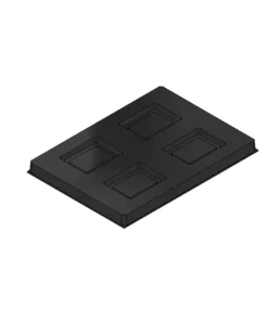
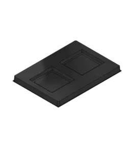

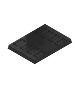

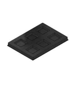
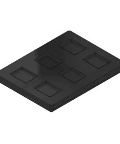
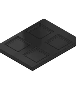
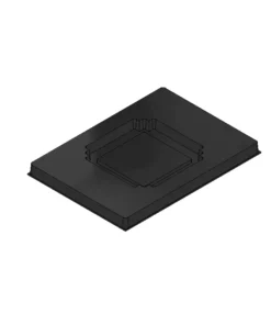
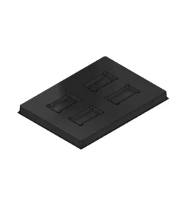
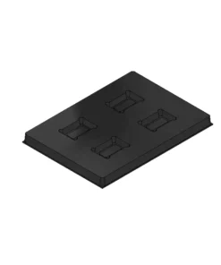
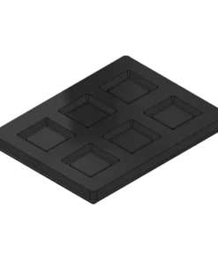
Conductive Device Inserts for Semiconductor Packaging
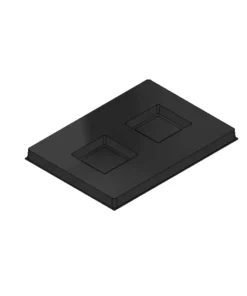
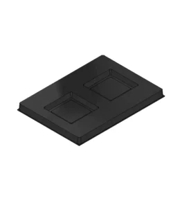
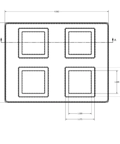
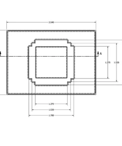
Malaster conductive device inserts help position semiconductor packages inside compatible protective boxes. Select an insert by its cavity geometry, device-contact arrangement, and intended box series. A general package label or similar nominal dimensions do not establish a correct fit.
Check the Device and Box Together
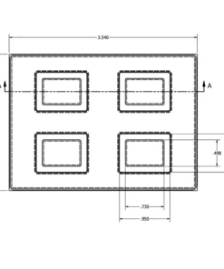
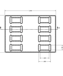
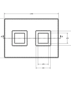
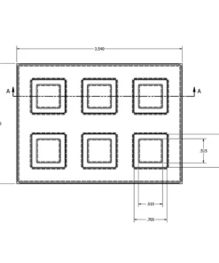
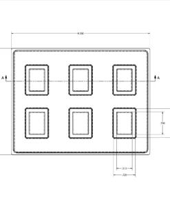
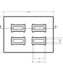
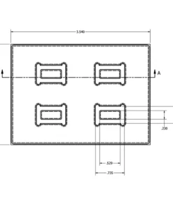
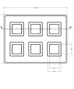
Compare the actual device body dimensions, lead or termination clearance, orientation, and permitted contact surfaces with the insert drawing.
Confirm the insert footprint and intended box series, including available height after the box is closed.
Review whether the selected configuration requires a top insert, cushion, or other retention component and whether those parts are supplied separately.
Confirm Material and Performance Requirements
Use the current product or material documentation to confirm construction, electrical properties, and applicable test conditions. Conductive material selection does not by itself establish the performance of the complete loaded package. Evaluate mechanical retention and ESD requirements for the intended process.
For particle-sensitive applications, review material contact, abrasion, and retention options before selecting foam or other internal components. Specify any required material or cleanliness documentation when requesting assistance.
See the device-insert selection guide for detailed fit guidance and compare the individual product listings below.