Compare tooling, materials, packing time, freight, and inventory to see whether custom packaging pays back for your application.

Category Archives: ESD Packaging Resources
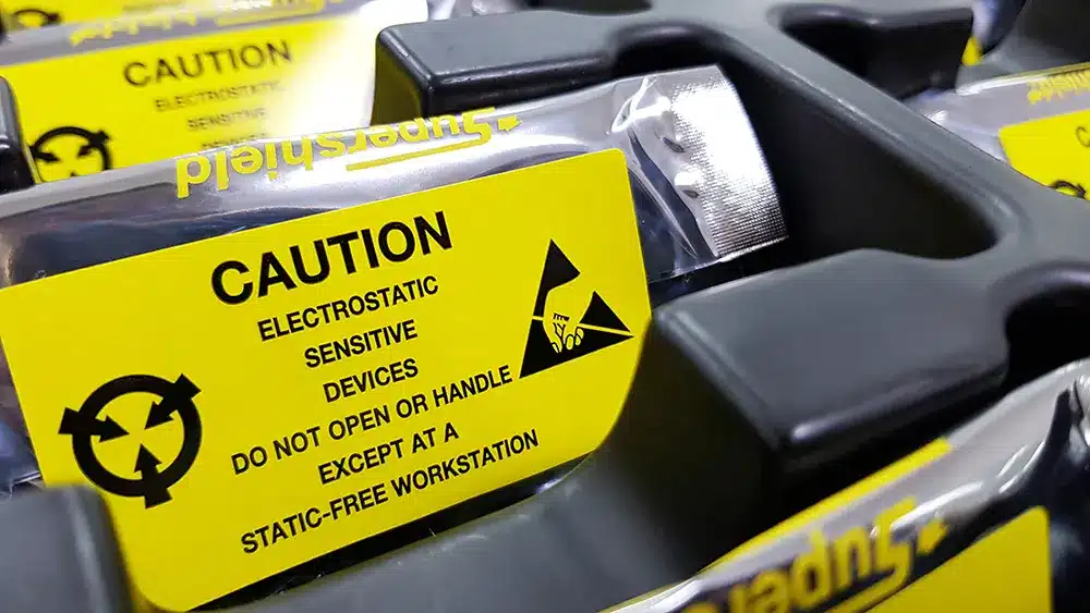
Educational articles covering ESD protection, semiconductor packaging, engineering best practices, and technical application guidance.
A receiving-to-storage checklist for inspecting packages, preparing the work area, transferring parts, and handling exceptions.
Apply component and handling requirements when choosing packaging for sensors, modules, and connected electronic assemblies.
Compare stock packaging, fitted inserts, and custom designs using component fit, handling, material requirements, and approval steps.
Understand stock and custom options, setup costs, selling units, sample approval, and scheduling for small packaging orders.
Compare low-charging, dissipative, conductive, and shielding materials, then select packaging for the component and handling environment.
Consider packaging cost alongside component protection, handling effort, and the requirements of the complete shipping system.
Evaluate packaging condition, qualification, return handling, and local disposal options before making reuse or recycling claims.
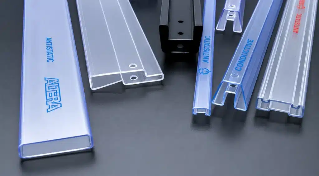
Review the role of tube profile, component support, closures, and electrical properties in IC handling and packaging.
An introduction to JEDEC tray formats and component handling, with practical tray identification and selection resources.