Category Archives: Packaging Design

Design principles, engineering considerations, dimensional analysis, and packaging development methodologies for semiconductor protection.

How to Specify a Custom ESD Foam Insert for Electronic Components
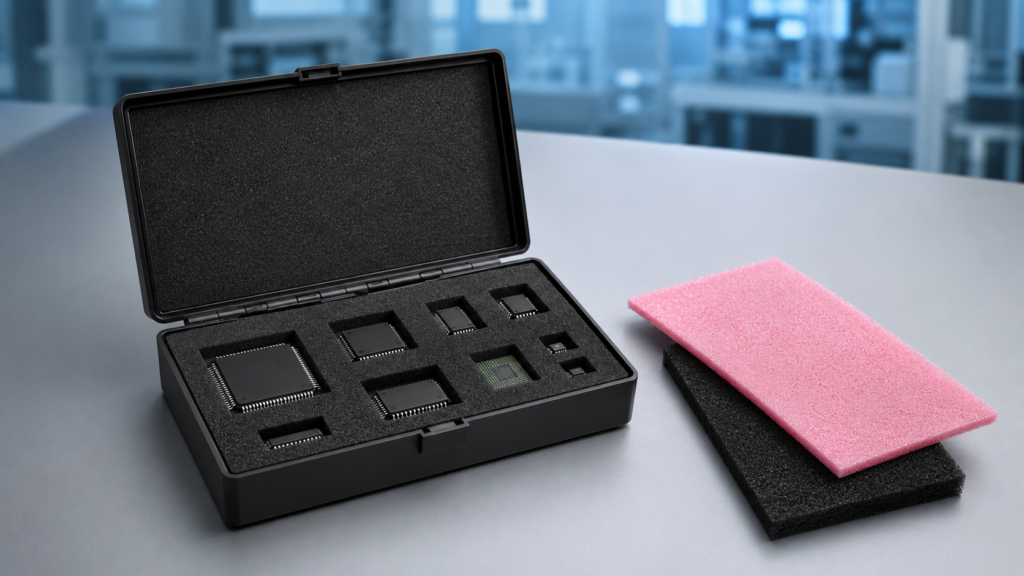
Electronic components secured in a custom conductive foam insert beside pink antistatic and black conductive foam samples

Custom Foam Insert Specification A custom ESD foam insert should be designed around the component, the surrounding package and the work the foam must perform. Start with a drawing, CAD file, sample or accurate dimensions. Identify delicate features and surfaces that need clearance, provide the available box space and quantity, and include any defined electrical […]

Reducing Costs with Custom Packaging Solutions

Optimize Cash Flow with Custom Packaging Solutions from Malaster During High Inflation Managing cash flow efficiently is crucial, especially during times of high inflation. One effective way to achieve this is by utilizing custom packaging solutions. Malaster specializes in providing tailored packaging options, ensuring that you receive the exact quantity you need, thus minimizing waste […]

Customizing ESD Protection

Custom ESD packaging and protection solutions for electronic components

Custom ESD Protection Solutions for Unique Electronics Applications Electrostatic discharge protection requirements can vary significantly depending on the electronic component, handling process, storage conditions, and shipping environment. While standard ESD products can support many applications, some situations require custom ESD protection solutions designed around specific operational needs. Why Custom ESD Protection Matters Custom ESD protection […]