

Start With the Package Family
Browse Tube Profiles by Device Style
These groups narrow the search, but they do not replace dimensional verification. Two components sold under the same package designation can differ enough in body or lead geometry to require different tube profiles.
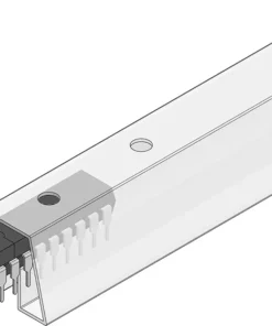
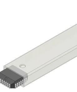
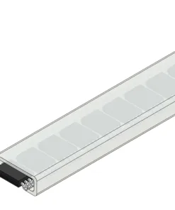
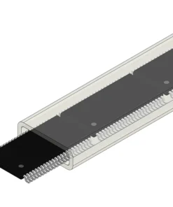
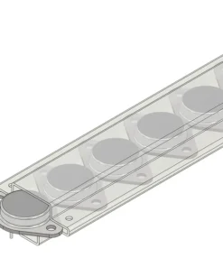
DIP / OptoThrough-hole and optoelectronic package profilesSOIC / SOJSmall-outline gull-wing and J-lead packagesSOP / TSOP / TSSOPThin and shrink small-outline package familiesPLCC / LCCLeaded and leadless chip-carrier profilesQFNNo-lead packages requiring controlled body supportTO / Socket CarrierSpecialized profiles for round and carrier-style devices
Need a profile match? Send the manufacturer package drawing or the actual body and lead dimensions. Malaster can compare them with established profiles before custom tooling is considered.
Selection and Application Guidance
A Tube Profile Is Only One Part of the Packaging System
Verify the cavityUse the product drawing and actual device dimensions to evaluate body and lead clearance. A package name alone does not establish compatibility.
Control unused lengthPins, plugs and filler can close the tube and manage movement when the tube is not loaded to its full usable capacity.
Protect the shipmentFor shipping, tube bundles should be restrained inside an appropriate outer package with the required ESD and cushioning controls.
Established profiles, low-quantity supply and custom lengthsMalaster maintains a broad catalog of semiconductor shipping-tube profiles and supports low-quantity requirements as well as production-volume supply. Existing profiles can also be cut to application-specific lengths.
Request Application Assistance →