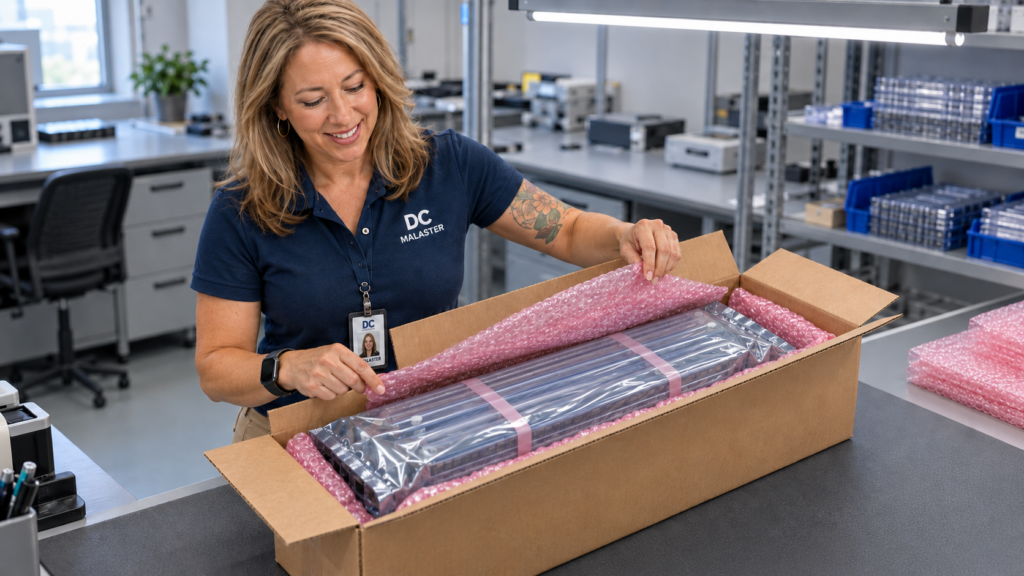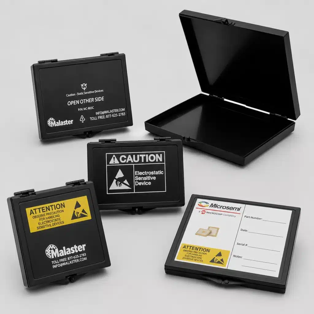
From DC’s packing bench at Malaster A neatly packed box is satisfying. Before the tape goes on, though, I want to know what is happening inside it: how the components are supported, what touches them, and whether that protection will hold up through shipping and unpacking. Shipping electronic components takes more than a snug carton. […]
Category Archives: Featured
Curated technical resources selected by Malaster to highlight important engineering guidance, new developments, and practical semiconductor packaging solutions.
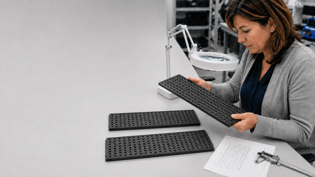
Malaster shares the practical process she uses to identify an existing JEDEC tray, verify revisions and temperature requirements, and gather the details needed to find the right replacement or new tray.
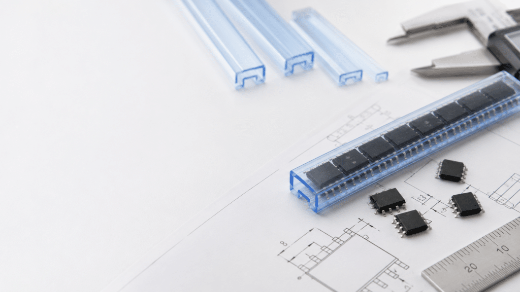
Most engineers start by asking which IC shipping tube fits their device. The better question is whether a tube is the right packaging solution at all. Learn how mechanical drawings, device geometry, ESD protection, and decades of engineering experience lead to better packaging decisions.