Guide
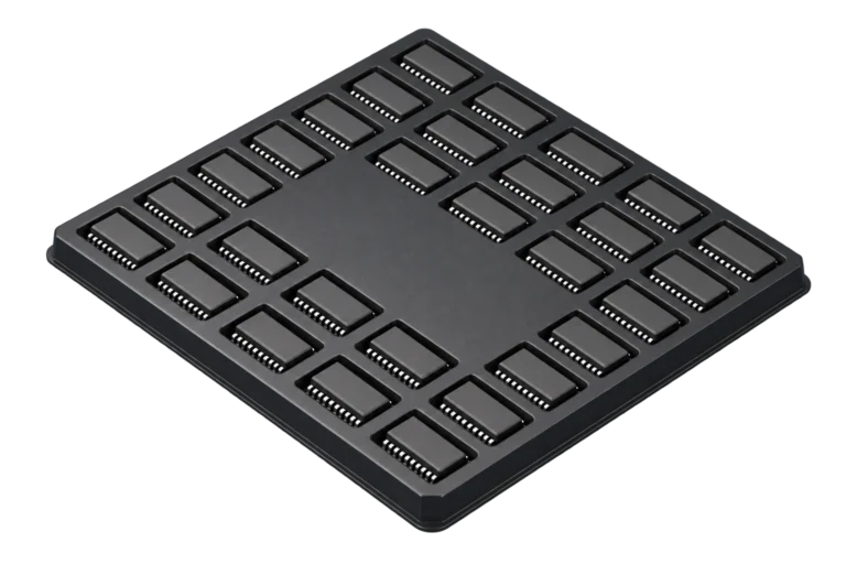
How to Choose a Thermoformed Tray for Electronic Components
Five checks for cavity fit, device support, handling, material thickness, and the loaded tray assembly.
View resource
Find practical packaging guidance, company stories, and the people behind Malaster. Browse by topic or explore the full library.
Choose a tube, check device fit, and plan closures and shipping.
5 resources
Mike Cordingley explains how package geometry, lead clearance, orientation, closures, and handling determine the right IC tube.
See why exposed SOIC leads need mechanical support as well as ESD protection during handling and shipment.
Five checks from the packing bench: movement, ESD protection, retention, bag closure and labeling, and the complete shipping package.
Review IC tube profiles, device support, materials, closures, and shipping requirements in the complete technical guide.
Review the role of tube profile, component support, closures, and electrical properties in IC handling and packaging.
Identify a tray, compare supply options, and review fit and handling.
5 resources
Melissa explains how she uses tray markings, drawings, pocket details, and samples to identify JEDEC trays and check component fit.
Find practical answers about JEDEC tray selection, identification, replacements, temperature, reuse, and requesting assistance.
Compare new and requalified JEDEC trays by condition, application requirements, documentation, and available supply.
Explore JEDEC tray dimensions, pocket geometry, materials, ESD properties, inspection, cleaning, reuse, and sourcing.
An introduction to JEDEC tray formats and component handling, with practical tray identification and selection resources.
Review custom tray design, materials, cavities, and packaging formats.
4 resources
Five checks for cavity fit, device support, handling, material thickness, and the loaded tray assembly.
Explore thermoformed tray design, materials, cavity geometry, manufacturing considerations, and application review.
Compare IC tubes, JEDEC trays, thermoformed trays, and ESD box systems by device fit, handling, and packaging requirements.
Compare stock packaging, fitted inserts, and custom designs using component fit, handling, material requirements, and approval steps.
Plan the jar, foam cushions, separators, and fit as one assembly.
1 resource
Configure wafer jars with foam cushions and separators, including stack height, custom shapes, and fit checks.
Compare box systems and foam materials, or specify a fitted insert.
3 resources
Review ESD box materials, foam and formed inserts, contact areas, cleanliness, printing, and discharge-shielding requirements.
Specify an ESD foam insert with clear dimensions, approved contact areas, material properties, package space, and cutting requirements.
Compare pink antistatic and black conductive foam, including cushioning, electrical behavior, contact areas, and application requirements.
Choose among antistatic, static-shielding, and moisture-barrier bags using the handling environment, sizing, and closure requirements.
See why exposed SOIC leads need mechanical support as well as ESD protection during handling and shipment.
Review band specifications, sizing, electrical terminology, and retention.
3 resources
Compare pink MC-ASRB and black MC-CRB specifications, lay-flat sizing, bag quantities, storage, and package retention checks.
Understand the electrical terminology used for black ESD rubber bands and the specifications that matter when selecting them.
Where ESD retention bands fit in tube bundles, tray stacks, and packaging, with links to current specifications and sizing guidance.
Understand ESD materials, packaging standards, receiving, and handling.
8 resources
Understand what electrostatic discharge is, how it affects electronics, and where protective packaging fits into static control.
A detailed reference on electrostatic discharge, protective materials, handling controls, packaging selection, and verification.
Understand ESD program and packaging standards, supplier evidence, and the difference between compliance and certification.
Questions to ask before adopting a new material or handling technology, from measured properties to process qualification.
A receiving-to-storage checklist for inspecting packages, preparing the work area, transferring parts, and handling exceptions.
Apply component and handling requirements when choosing packaging for sensors, modules, and connected electronic assemblies.
How conductive, static-dissipative, and low-charging properties differ, and why material labels alone do not establish shielding.
An introduction to ESD packaging and the handling controls that protect sensitive electronics during storage and shipment.
Compare formats, plan custom work, evaluate costs, and prepare a request.
11 resources
Compare IC tubes, JEDEC trays, thermoformed trays, and ESD box systems by device fit, handling, and packaging requirements.
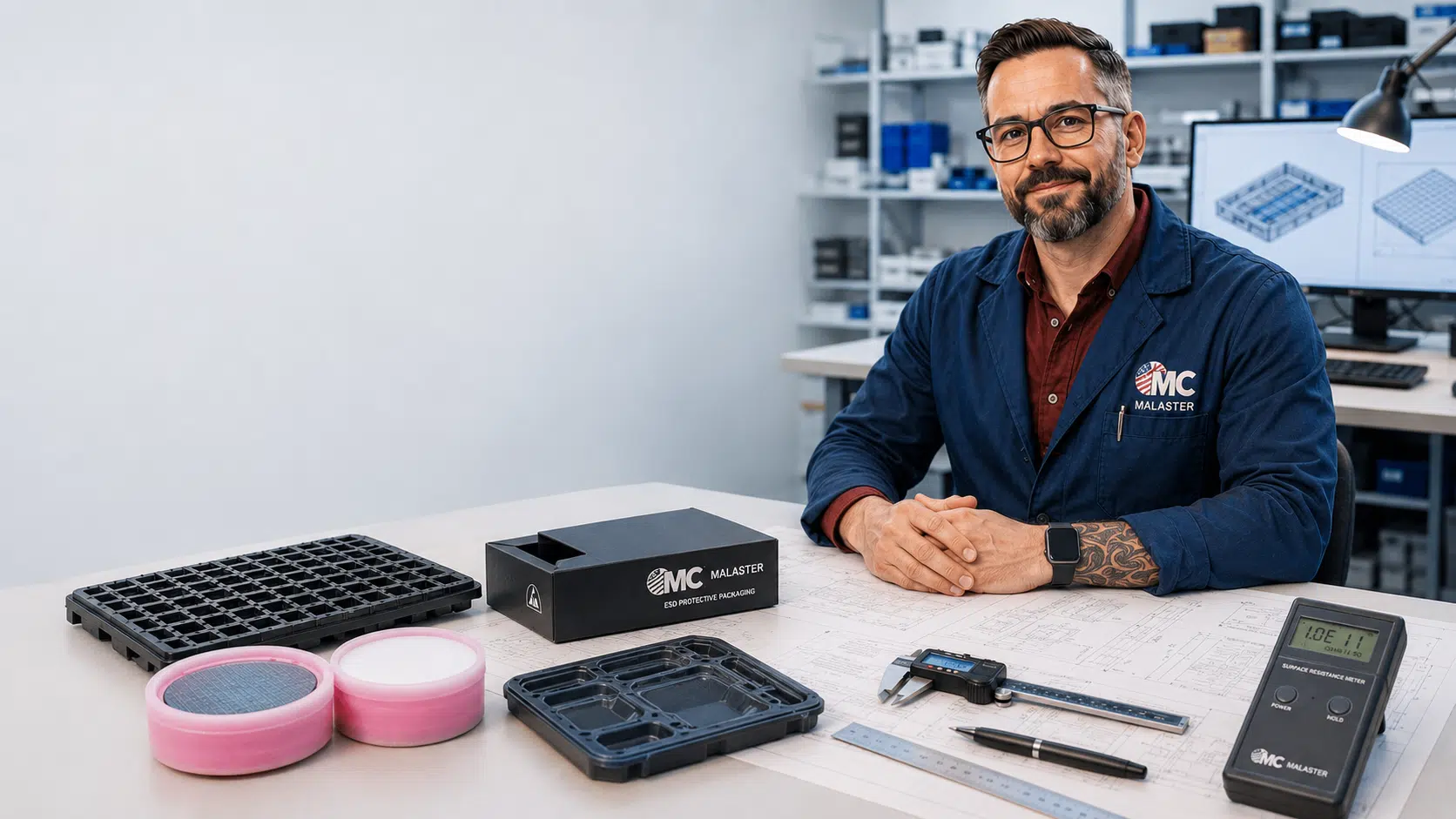
Denise Cordingley shares how clear questions, realistic expectations, and ongoing communication help customers and packaging suppliers work better together.
How component details, handling conditions, and packaging requirements guide a useful technical discussion with Malaster.
Information to bring to a packaging review and the support available for standard and custom electronics packaging.
Compare tooling, materials, packing time, freight, and inventory to see whether custom packaging pays back for your application.
Compare stock packaging, fitted inserts, and custom designs using component fit, handling, material requirements, and approval steps.
Understand stock and custom options, setup costs, selling units, sample approval, and scheduling for small packaging orders.
Compare low-charging, dissipative, conductive, and shielding materials, then select packaging for the component and handling environment.
Consider packaging cost alongside component protection, handling effort, and the requirements of the complete shipping system.
Evaluate packaging condition, qualification, return handling, and local disposal options before making reuse or recycling claims.
When component geometry and handling requirements call for a fitted insert, different carrier, or custom packaging review.
All published articles and technical guides, newest first. New resources appear here as they are published.
Guide
Five checks for cavity fit, device support, handling, material thickness, and the loaded tray assembly.
View resource
Article
Denise Cordingley shares how clear questions, realistic expectations, and ongoing communication help customers and packaging suppliers work better together.
View resource
FAQ
Find practical answers about JEDEC tray selection, identification, replacements, temperature, reuse, and requesting assistance.
View resource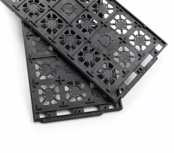
Guide
Compare new and requalified JEDEC trays by condition, application requirements, documentation, and available supply.
View resource
Guide
See why exposed SOIC leads need mechanical support as well as ESD protection during handling and shipment.
View resource
Article
Five checks from the packing bench: movement, ESD protection, retention, bag closure and labeling, and the complete shipping package.
View resource
Guide
Configure wafer jars with foam cushions and separators, including stack height, custom shapes, and fit checks.
View resource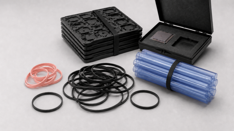
Guide
Understand the electrical terminology used for black ESD rubber bands and the specifications that matter when selecting them.
View resource
Guide
Understand what electrostatic discharge is, how it affects electronics, and where protective packaging fits into static control.
View resource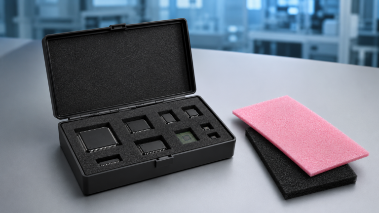
Article
Specify an ESD foam insert with clear dimensions, approved contact areas, material properties, package space, and cutting requirements.
View resource
Article
Compare pink MC-ASRB and black MC-CRB specifications, lay-flat sizing, bag quantities, storage, and package retention checks.
View resource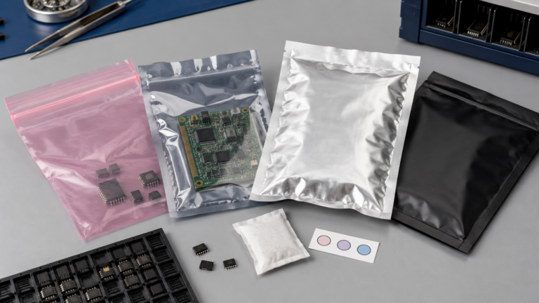
Guide
Choose among antistatic, static-shielding, and moisture-barrier bags using the handling environment, sizing, and closure requirements.
View resource
Guide
Compare pink antistatic and black conductive foam, including cushioning, electrical behavior, contact areas, and application requirements.
View resource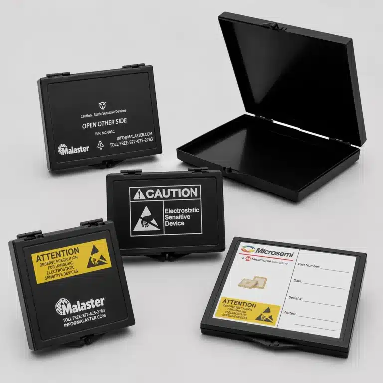
Article
Review ESD box materials, foam and formed inserts, contact areas, cleanliness, printing, and discharge-shielding requirements.
View resource
Article
Melissa explains how she uses tray markings, drawings, pocket details, and samples to identify JEDEC trays and check component fit.
View resource
Guide
Explore JEDEC tray dimensions, pocket geometry, materials, ESD properties, inspection, cleaning, reuse, and sourcing.
View resource
Guide
Explore thermoformed tray design, materials, cavity geometry, manufacturing considerations, and application review.
View resource
Guide
A detailed reference on electrostatic discharge, protective materials, handling controls, packaging selection, and verification.
View resource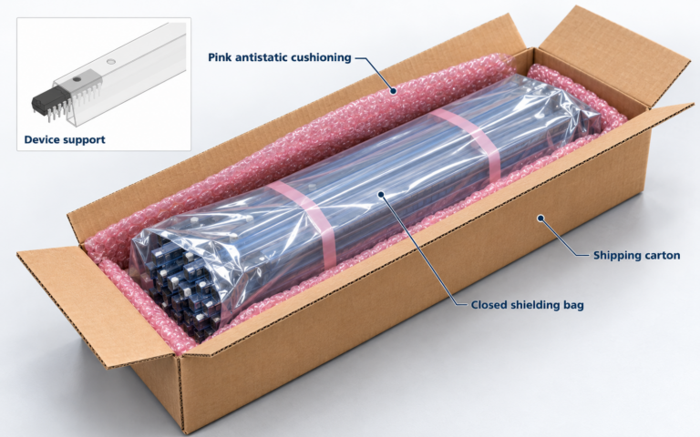
Guide
Review IC tube profiles, device support, materials, closures, and shipping requirements in the complete technical guide.
View resource
Article
Mike Cordingley explains how package geometry, lead clearance, orientation, closures, and handling determine the right IC tube.
View resource
Article
Compare IC tubes, JEDEC trays, thermoformed trays, and ESD box systems by device fit, handling, and packaging requirements.
View resource
Article
Understand ESD program and packaging standards, supplier evidence, and the difference between compliance and certification.
View resource
Article
How component details, handling conditions, and packaging requirements guide a useful technical discussion with Malaster.
View resource
Article
Questions to ask before adopting a new material or handling technology, from measured properties to process qualification.
View resource